

Find the right way to clean nanocrystals is harder than it looks
|Due to their intense photoluminescence and remarkable tolerance to defects, nanocrystals of CsPbBr3 (a type of halogenated inorganic perovskite) are among the best candidates for next-generation LEDs, solar cells, and photodetectors. But paradoxically, making them truly useful relies only on an apparently simple step: cleaning them.
This is because directly after synthesis, these nanocrystals are actually coated with long organic ligands that keep them stable in solution. However, removing excess ligands is essential because too many act as insulating barriers, preventing charge transport in devices. Yet removing the ligand shell entirely destabilises the crystals, which eventually introduces defects and degrades performance.
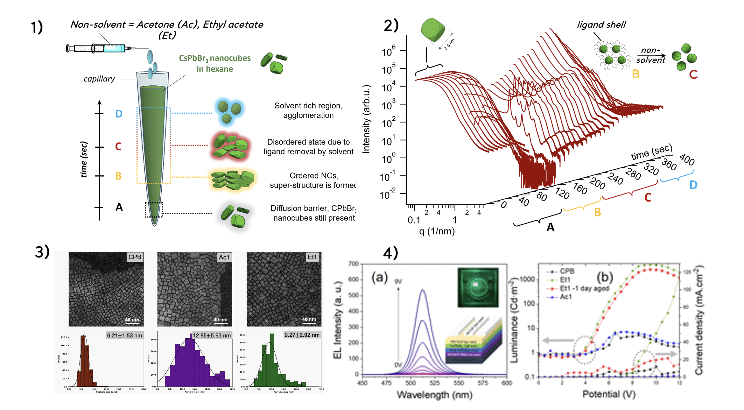
Bapi Pradhan (KU Leuven), Sumea Klokic (CERIC post-doc, now researcher at TU Graz) and colleagues analysed this delicate balance by comparing two common nonsolvents: acetone and ethyl acetate. Using a combination of advanced analytical techniques – such as transmission electron microscopy, nuclear magnetic resonance, and in situ small-angle X-ray scattering available at CERIC Austrian Partner Facility – researchers studied how the purification process reshapes both structure and dynamics of nanocrystal. Standard optical measurements suggested little difference between treatments. However, deeper analysis revealed that acetone, the more polar solvent, strips the ligands aggressively, creating structural defects and inducing blinking and photobleaching at the single-particle level. Ethyl acetate, on the other hand, enables gentler ligand exchange and preserves structural integrity.
The impact is evident in devices performance: LEDs made from ethyl acetate-treated nanocrystals achieved over twice the efficiency compared to acetone-treated ones. The takeaway is clear: nanocrystal purification is not just a cleanup step, but a critical design parameter that governs performance of next generation devices at every scale.
ORIGINAL ARTICLE: