

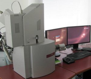
LYRA dual focused Ion Beam Scanning Electron Microscopy (FIB-SEM)
Charles University in Prague
Focused Ion Beam Scanning Electron Microscopy (FIB-SEM) has become an essential tool for materials science and engineering. It is a technology developed from the simpler form of SEM (Scanning Electron Microscopy). The difference between SEM and FIB is that the beam of electrons that is used in SEM for imagining of the sample surface is replaced by a focused beam of ions.
In FIB, a finely focused beam of ions (usually gallium) can be operated at low beam currents for imaging or at high beam currents to directly affect the surface of a sample, i.e. for site specific sputtering or milling.
A FIB becomes a powerful tool when it is combined with an SEM, where a dual electron beam intersects the ion beam at a 55° just above the sample surface, enabling simultaneous SEM imaging of the surface milled by FIB. Such a configuration in dual beam systems ensures high level of precision in all FIB milling tasks (micro/nanomachining/nanopatterning).
A FIB-SEM can also be used to deposit material via ion/electron beam induced deposition by scanning an area with the beam, when a gas precursor is introduced to the vacuum chamber by using Gas Injection System (GIS). Almost any shape can be deposited, either using the shapes and text provided by the software or importing an image.
GIS provides precursor reactive gas sources to deposit material, to reduce charging effect from both electron and ion beams, to assist in enhanced etching and to protect the sample and reduce curtaining effects on the cross-section during ion beam milling.
The method has been widely adopted in the fields of semiconductor and electronic development, materials science, biology, neuroscience, and more.
Contact:
Prof. Iva Matolínová (tel:+420-95155-2241)
Dr. Jaroslava Nováková (tel:+420-95155-2251)
Technical specifications
LYRA I FE XMH
(Extra Large Chamber, Extended Motorized Stage, High Vacuum Operation)
A fully PC controlled SEM with Schottky field emission cathode in combination with gallium Focused Ion Beam (FIB) column and with Gas Injection System (GIS) suitable especially for the preparation of samples in the form of thin lamellae for TEM observation.
Electron Beam Column:
Magnification: 3´ – 1,000,000´
Accelerating Voltage: 200 V to 30 kV
Resolution: 2 nm and 4.5 nm (depending on configuration and accelaration voltage)
Ion Beam Column:
Magnification: 150´ – 1,000,000´
Accelerating Voltage: 1 kV to 30 kV
Ion Gun: Ga Liquid Metal Ion Source
SEM-FIB Coincidence at: WD 9 mm for SEM – WD 12 mm for FIB
SEM-FIB angle: 55°
Gas Injection System:
5 independent gas reservoirs with capillaries for:
- Tungsten metal deposition
- Platinum metal deposition
- Insulator (SiOx) deposition
- Enhanced etching of diamond and PMMA (H2O)
- Enhanced or selective etching of Si, SiO2, Si3N4, W (XeF2)
3-axis microstage with automatic nozzles positioning
Automated temperature control
Detectors:
SE – Secondary electron detector Everhardt-Thornley type (YAG Crystal)
BSE – Retractable annular scintillator type (YAG Crystal) with high sensitivity and atomic number resolution (0.1)
EDX – – Take off angle 35° at SEM WD 9mm (coincidence point)
Sample requirements
The samples must be high vacuum stable and conductive.
Detailed information can be found on the instrument’s webpage.